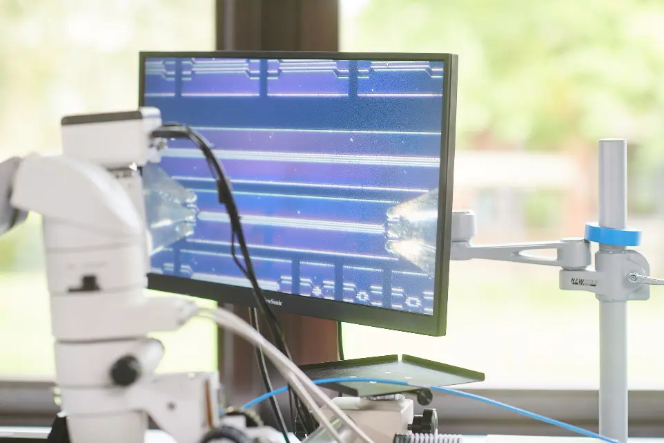
Electrical Characterization Services
Materials and Substrates
We helped develop every existing RF substrate.


Devices and Circuits
We test it before it goes into your phone.


Material Characterization
Oxide-substrate charges
Flatband capacitance and voltage
Oxide thickness
Effective & total bulk oxide charge
Substrate doping concentration
Dielectric
Permittivity
Loss tangent
Four point probe
Sheet resistance
Bulk resistivity

Substrate Characterization
We have unique know-how in characterization of Si and SOI substrates including high resistivity and trap rich materials.
We develop the adequate design of test structures in order to create the most accurate picture of the behavior of the substrate in different operation conditions.

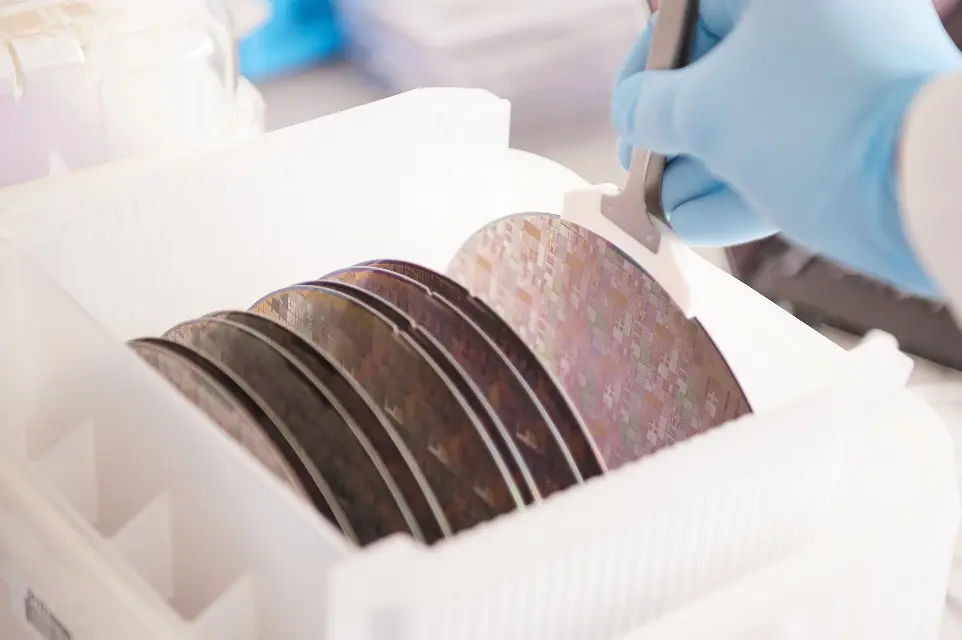
Materials and Samples
Materials
Silicon: Bulk, SOI, Trap-Rich, Porous, SiC, SiGe ...
III-V: GaN, GaAs ...
Dielectric: Quartz, Fused Silica ...
Piezo: LiTaO3, LiNbO3, ZnO ...
2D: Graphene, hBN ...
Phase-changing: VO2, GeTe ...
Samples
Size: from a single die to 300 mm wafer
Shape: Piece of wafer or whole wafer

RF Characterization
Large signal
- Harmonics (single tone), intermodulation (dual tone) and power handling
- Input power up to 49 dBm
- Noise floor -170 dBm
Small signal
- S-parameters up to 170 GHz
- Low frequency from 5 Hz
- RF figures of merit
5G mm-wave
- Small- and large-signal
- Adapted calibration techniques
- Application specific
Noise Measurements
RF thermal noise
- 1 – 110 GHz
- Down to 0.2 dB of NFmin
- Programmable microwave tuners
- Measurement of NFmin, Rn, Yopt and NF50
1/f flicker noise
- Frequency range from of 0.03 Hz to 40 MHz
- Noise measurement down to 0.67 nV/sqr(Hz) @ 10 kHz
- 25 impedance values ranging from 0 ohms to 100 MΩ
- Current/voltage/power range of up to 0.1 A/200 V/10 W, respectively
- Supported devices include BJTs, FETs, diodes, resistors and circuits (op-amps, comparators, etc.)
Random telegraph signal noise (RTS, RTN)
- Time domain representation of noise
- Current and voltage histograms
- Supported devices include BJTs, FETs, diodes, resistors and circuits (op-amps, comparators, etc.)
- 2.5 ns minimum time step
- Sampling size up to 16 million


Cryogenic Measurements
Temperature
- Cryogenic from -270°C (4 K)
- Hot chuck up to 225°C
RF Signal
- S-parameters up to 67 GHz
- Low frequency from 5 Hz
- RF figures of merit
DC and AC
- Pulsed IV down to 100 ns pulse width
- Ultra low voltage and current
- CV measurements
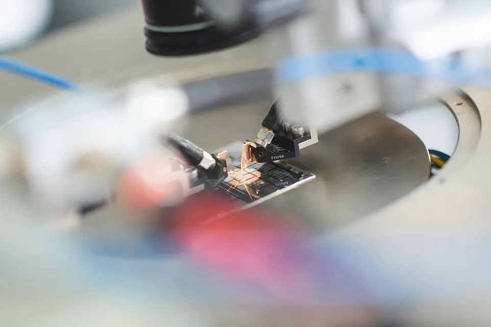
Facility
WELCOME is a state-of-the-art facility offering a complete characterization service solutions. Incize is a privilege partner and collaborator of this facilities. Experts from Incize excelle on a daily basis in offering top-notch testing services using the latest and most advanced equipments available in this facility, while introducing innovative solutions beyond the limits of commercial equipments.
Questions?
Embark with us on a journey to build technology for future generations
Join us and make tomorrow's technology possible.