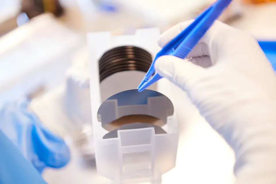
Cleanroom Services
We develop your innovative process steps
Our talented process team help develop and optimise state-of-the-art process steps giving you an edge on the technology and reduce time-to-market cycles.

Services
Metallization
Wet & dry etching
Photo & e-beam lithography
Laser & FIB
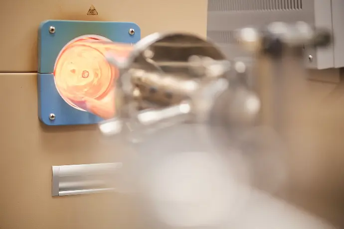
Sputtering & thermal deposition
PCD, PECVD, LPCVD & ALD
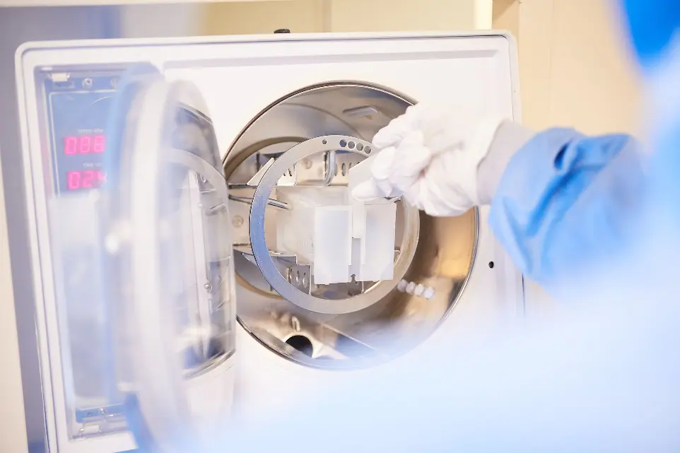
Back-end process & packaging
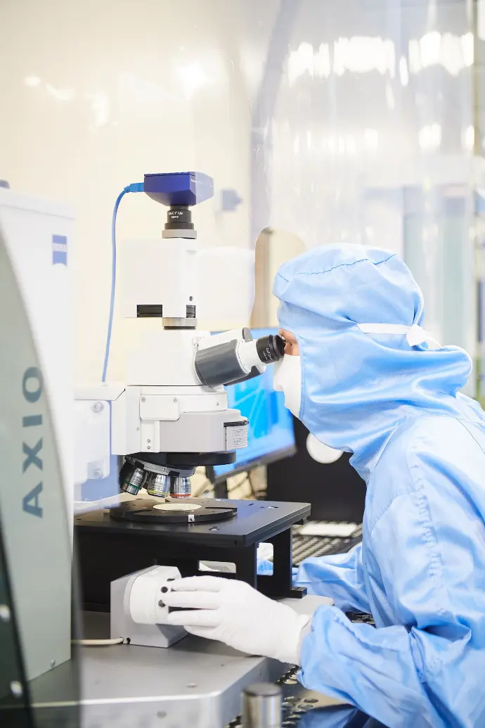
SEM, TEM, profilometry, nanoindentation

Materials
Substrates: Si, III-V, porous, quartz, ...
Metals: Al, Ag, Au, Ti, Ni, Cr, Pd, ...
Dielectrics: Si3N4, SiO2, Al2O3, TiO2, HfO2, …
Polymers
Samples
Shape: from wafer to piece of wafer
Size: from die to 8 inches
Facility
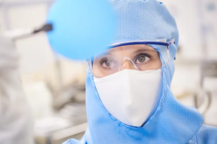
WinFAB is the cleanroom of UCLouvain and house of esteemed reputation of expertise and innovation.
Area: 1000 m²
Class: < 10 particles of100 nm/feet³ of air
Equipment: 50 advanced R&D cleanroom equipment
Tools: surface-patterning, thin films deposition and etching & back-end processes
Activities: SOI-CMOS, thin film characterization, co-integration, photovoltaic, MEMS-NEMS, sensors, bio-technologies, porous Si, organic electronics & nano-electronics
Questions?
Embark with us on a journey to build technology for future generations
Join us and make tomorrow's technology possible.