Optical characterization
Raman

- High resolution confocal microscope
- 800 mm focal length
- Lateral resolution below 1 μm
- Laser wavelengths 458, 488, 514 & 633 nm
- Temperature -196°C ... +600°C
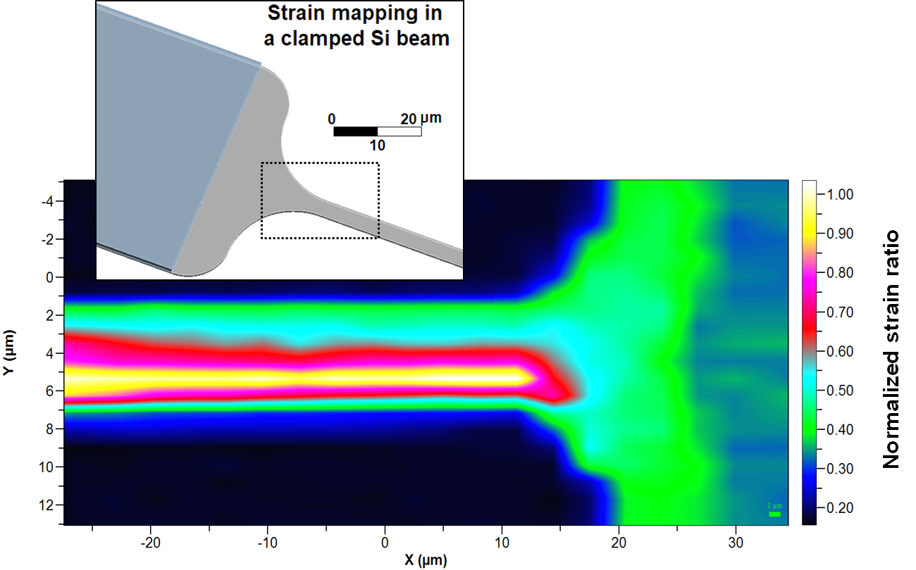
- Mapping analysis including chemical composition, phase, crystallinity and strain
Read more Raman spectroscopy is an optical non-destructive characterization technique used to analyze numerous materials including semiconductors and thin films with none or minimum sample preparation. The information obtained is extremely rich and can be used to identify material composition, stress and strain, doping concentration and phase formation. Since the discovery of the Raman effect in 1928 by Sir C.V. Raman [1], the advance in laser technology and fabrication of high selective filters has permitted a rapid development in Raman instrumentation. Today, the use of high resolution lenses, gratings and detectors allows the characterization of the Raman effect in structures and materials down to micrometer and nanometer size. New to our customers, Incize provides high resolution Raman spectroscopy for the characterization of materials and samples with spatial resolution down to ~1 μm. Equipped with four laser wavelengths, 458, 488, 514 and 633 nm and a motorized stage in x-y-z, we can perform micro-Raman analysis such as chemical composition, phase, crystallinity and strain in numerous materials including those most used in the semiconductor industry (Si, Poly-Si, Ge, SiGe, GaN), 2D materials (graphene, hBN), phase transition materials (VO2, V2O5, GeTe) and piezoelectric materials (LiNbO3, LiTaO3, ZnO). We also offer the possibility of performing Raman-temperature measurements in the range -196°C to 600°C. [1] C.V. Raman and K.S. Krishnan, “A new type of secondary radiation”, Nature, vol. 121, pp. 501–502, 1928
Photoconductance

- Photoconductance and resistivity measurements of Si photovoltaic
2 ... 1000 Ω/□ - Minority carrier density and lifetime
100 ns ... 10 ms - QSS for short carrier lifetimes
- TPCD for long carrier lifetimes
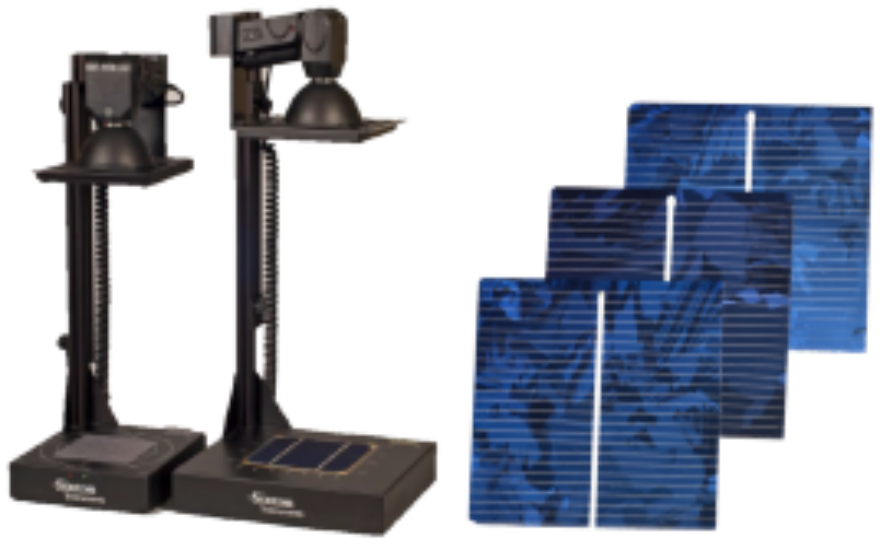
Read more Photoconductivity is a property of some materials in which a change in their electrical conductivity occurs in response to the absorption of light. In a typical photoconductance experiment, excess free carriers are generated by illuminating a sample with light from a laser source or a flash lamp. The technique is especially suitable for measuring the photoconductance and resistivity of silicon photovoltaic wafers ranging from 2 to 1000 Ω/□ and also to extract the minority carrier density and minority carrier lifetimes (100 ns < τ < 10 ms). Several types of light exposition are available depending on the range of resistivities and carrier lifetimes to be measured including constant light exposition (steady-state), light pulse (transient decay), or time varying light intensity (quasi-steady-state).
Ellipsometry

- Broad spectral range 280 ... 2500 nm
UV / Vis / NIR - Accurate film thickness analysis
single and multiple layered samples - Characterization of optical parameters
including refractive index, extinction
coefficient and dielectric function - Large range of materials: insulators (SiO2 , Si3N4 ), semiconductors (Si, Ge, SiC) and metals (Al, Ag, Au, Cu, Cr)
Read more Ellipsometry is a non-destructive optical technique which measures the relative change in the polarization state between the incident light and that reflected in a thin film or a layered material for a specific angle. By using appropriate fitting models for the measured spectra, several material parameters such as the layer thickness, index of refraction and the optical absorption and extinction coefficients can be determined. Ellipsometry measurements are very precise and depending on the material, thicknesses ranging from a few Armstrongs to a few micrometres can be measured. A large range of materials including most insulators (SiO2, S3N4,…), semiconductors (Si, Ge, SiC,…) and metals (Al, Ag, Au, Cu, Cr,…) can be characterized using light wavelengths ranging from 280 to 2500 nm (UV / Vis / NIR).

